
Types of Signals Does an RF Board Handle
The circuit boards that are used to house the wireless signal processors and other critical components in a mobile phone or tablet are known as RF (radio frequency) boards. These boards handle signals for cellular networks like 2G, 3G, 4G, 5G and Wi-Fi as well as NFC, Bluetooth and other wireless communication protocols.
Unlike traditional PCBs, RF boards require specific materials that meet high-frequency operation requirements. These materials must be able to transmit signals over long distances without interference, while also offering stability at high frequencies. Additionally, the layout of RF traces must be carefully considered to maximize performance. This requires careful consideration of trace width, spacing and impedance matching.
In order to maintain proper signal integrity, a rf board must have a ground plane and power plane. Keeping the two separate reduces parasitic capacitance and inductance that can affect circuit performance. It’s also important to maintain consistent impedance throughout the PCB traces and transmission lines. This helps to minimize signal reflections and improves overall performance.
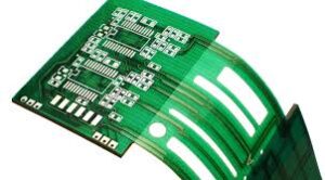
What Types of Signals Does an RF Board Handle?
When it comes to designing an RF circuit board, it’s essential to take into account the different factors that differentiate them from standard PCBs. For example, RF circuits must have very tight trace widths and spacing to reduce crosstalk between the individual traces on the board. Additionally, RF traces must be designed with larger bend radiuses to accommodate for the increased frequencies of these signals. This ensures that the traces can withstand the higher voltages and frequencies that are associated with these signals.
The material of an RF circuit board is another critical factor that distinguishes it from other PCB designs. It must meet the necessary performance standards for RF and microwave operations, including low signal loss, stable operation at high frequencies and the ability to absorb large amounts of heat. For these reasons, most RF circuit boards are made of polytetrafl uoroethylene (PTFE), ceramics or hydrocarbons mixed with PTFE or a form of glass.
RF PCBs are typically tested using methods such as S-parameters to determine their performance. This process allows designers to catch any potential issues early on and make adjustments before the product goes into production. It also enables them to optimize the design so that it performs as expected and meets all of the design criteria for the given application.
In satellite communication, RF boards facilitate the transmission of signals to and from satellites orbiting the Earth. These boards must endure extreme environmental conditions, such as high radiation levels and temperature fluctuations.
RF PCBs are an essential part of today’s technology and they help to enable the wireless connectivity in many of our most popular devices. However, it’s important to remember that these boards are designed and built for specific applications and that they must be tailored to meet the unique requirements of each. This includes the use of specialized materials, proper impedance matching and careful component placement to avoid noise and interference. Taking the time to understand these factors and how they apply to a given application can help engineers create a successful RF PCB that delivers optimal performance.