
PCB Board Fabrication
PCB (Printed Circuit Board) fabrication is a fundamental process in the manufacturing of electronic devices. As the backbone of nearly every electronic product, from smartphones to medical equipment, PCBs play an essential role in connecting and supporting electronic components. The fabrication of PCB boards involves a series of highly precise steps that require attention to detail, advanced technology, and thorough testing. In this article, we will delve into the various stages of PCB board fabrication and their significance in ensuring a functional and reliable circuit board.
The first step in pcb board fabrication is the creation of the design. Engineers use specialized computer-aided design (CAD) software to develop the layout of the PCB, which includes placing the various electrical components and routing the necessary connections (traces) between them. The design file is then exported in a format that can be understood by the PCB manufacturer. One of the key considerations in this phase is the choice of material for the PCB. Most PCBs are made from fiberglass (FR4), though materials like aluminum or flexible substrates are used for specific applications. The choice of material impacts the PCB’s thermal conductivity, flexibility, and overall performance.
After the design has been finalized and the material chosen, the PCB fabrication process moves to the next stage: transferring the design onto the board. A copper-clad laminate, which consists of a thin layer of copper bonded to the base material, is used as the starting point. The first step involves cleaning the copper surface to remove any impurities, ensuring good adhesion of the subsequent layers. The design pattern is then transferred to the copper surface using photolithography, a process that involves applying a light-sensitive film to the board and exposing it to ultraviolet light through a mask. This process creates the desired pattern of copper traces on the PCB.
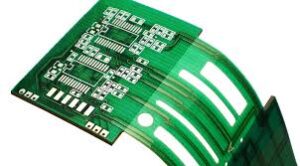
PCB Board Fabrication: Understanding the Crucial Manufacturing Process
Following the photolithography process, the PCB undergoes an etching procedure, which removes the unwanted copper from the board, leaving behind the desired circuit paths. This is typically done using a chemical solution, and the etching process requires precision to ensure that the traces are clear and free of any defects. In some cases, the etching process is done using laser etching, which offers high precision and reduces the risk of human error.
Once the copper traces are formed, the PCB is drilled to create holes for the components. For multi-layer PCBs, vias—small holes that connect different layers of the board—are drilled to ensure electrical continuity between the layers. These holes are usually drilled using a computer-controlled drilling machine, which ensures that they are placed with high accuracy. The size and placement of these holes are critical to the overall functionality of the PCB.
After drilling, the next step in the fabrication process is the application of a solder mask. The solder mask is a layer of protective material that is applied to the PCB to prevent solder bridges, which can occur during the assembly process when solder connects two adjacent pads unintentionally. The solder mask also helps protect the copper traces from environmental damage, such as oxidation. After the solder mask is applied, the PCB is printed with a silkscreen to label the component placement areas, making it easier for assembly technicians to know where each component should be placed.
Once the PCB has passed through all these processes, it is subjected to rigorous testing. This includes both visual and automated optical inspection (AOI) to detect any defects in the board, such as faulty traces, misalignment, or missing components. Electrical testing is also performed to verify that the PCB’s circuits function as intended. This testing ensures that the board will perform reliably in its intended application.
Finally, after passing all tests, the PCB is ready for shipment or further assembly, where components will be mounted and soldered onto the board. The fabrication of the PCB is a critical step in the electronics manufacturing process, as any error during fabrication can result in malfunctioning or unusable products.
In conclusion, PCB board fabrication is a highly detailed and technical process that is essential for the functioning of modern electronic devices. From the initial design to the final testing, each stage of the fabrication process ensures that the board meets the required specifications and performs reliably. As technology continues to evolve, so does the complexity of PCBs, with multi-layer boards, high-density interconnects (HDI), and flexible PCBs becoming increasingly common in advanced applications. Understanding the PCB fabrication process is crucial for anyone working in electronics manufacturing or design, as it forms the foundation for the entire electronics industry.