
HDI PCBs Are Used in High-Performance Computing
In a digital world that is becoming more and more complex, high-performance computing requires sophisticated hardware. HDI PCBs are ideal for this because of their increased circuit density, superior signal transmission quality, and reduced crossing delays. They can also support smaller component sizes and higher pin counts while reducing the overall footprint of the board, making them more compact than standard multi-layer PCBs.
In order to optimize the performance of HDI boards, it is necessary to understand how the board’s layers and components communicate with one another. Interconnections are what define a PCB’s functionality, and HDI design techniques maximize interconnectivity to improve the board’s performance and manufacturability.
HDI PCBs have more layers than standard multi-layer PCBs, allowing designers to include more components and achieve higher circuit density. However, despite their greater efficiency, they must be carefully designed to maintain signal integrity. This requires the shortest possible routing paths, consistent path impedance, adequate grounding layers, and the separation of digital, analog, and power signals.
To ensure that these requirements are met, it is important to use the right design tools. For example, you should be able to create an impedance profile and routing rules within your CAD software that will satisfy the fabrication fabricator’s DFM (Design for Manufacturing) guidelines. Additionally, you should be able to run a DRC engine to automatically check your routing as you build it.
High-speed signal testing is critical to verify that hdi board can meet the performance demands of high-speed electronic devices. It can help identify inconsistencies in impedance, which can degrade signal quality and increase energy loss. It also demonstrates that the materials used in HDI boards can withstand the higher data rates and RF frequencies required by modern electronics.
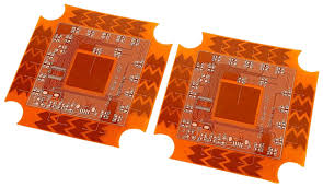
How HDI PCBs Are Used in High-Performance Computing
The use of blind, buried, and microvias in an HDI design helps to save space and enhance the board’s routing efficiency. However, using them too frequently can increase cost and lead to manufacturing challenges. The use of staggered microvias can also reduce the number of layers and help with signal flow.
Minimizing the layer count can also decrease manufacturing costs and simplify production. However, it is important to consider the thermal stability of your materials. Thin dielectric layers can become prone to stress during manufacturing and operation, especially when exposed to high temperatures or repeated soldering cycles. By choosing materials with a low coefficient of thermal expansion and good mechanical resilience, you can minimize these issues.
HDI PCBs are highly versatile and can be utilized in many different applications. They are a great choice for products that require improved connectivity and performance, such as touch screen computers and mobile devices. With the right engineering and manufacturing partner, you can achieve an optimal balance of performance, cost, and reliability. With a combination of careful material selection, optimized board layout, and cost-efficient manufacturing processes, HDI boards are an excellent solution for the most demanding electronics.
In telecommunications, HDI boards are used in devices like smartphones, tablets, and base station equipment. As the demand for higher-speed networks and more compact devices grows, the need for HDI boards continues to rise. The miniaturization of mobile devices, in particular, has driven the demand for HDI technology, as it allows manufacturers to pack more functionality into smaller spaces.