
manage signal integrity in a printed circuit prototype
Electronic devices rely on clear, high-speed signals to transmit data. However, these signals can be degraded by internal sources of interference or external sources such as electromagnetic fields. In order to minimize signal degradation, PCBs need to be designed with signal integrity in mind. This is especially important for high-speed digital systems such as cell phones and iPads, but also for medical equipment, aviation controls, robotics, and even brain chip implants.
Managing signal integrity in a printed circuit prototype involves designing the physical layout of a printed circuit board to mitigate the effects of signal attenuation, crosstalk, and ground bounce. This is done by laying out traces that meet certain width and spacing guidelines, while considering current carrying capacity and manufacturability. It also includes placing decoupling capacitors in the correct locations to manage power delivery and thermal management, as well as ensuring that the board is adequately shielded to prevent interference with sensitive components.
Many signal integrity problems are not apparent until a design takes a physical form. This is because a digital or analog circuit connection in software is represented by a simple line, but the actual connection on a physical board has an impedance that is influenced by track size and shape, spacing, copper layer thickness, the dielectric loss of the PCB material, and parasitic effects such as the effect of the trace on its surrounding metal pads. The result is that, without proper analysis using tools like SPICE and an oscilloscope, many signal power integrity and crosstalk problems go undetected until the prototype board is built and tested.
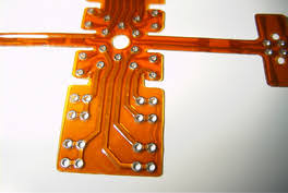
How do you manage signal integrity in a printed circuit prototype?
One of the main ways to avoid these issues is by routing all the cables in a way that reduces signal attenuation. This means keeping traces away from each other, as well as from power sources and all electrical fixtures. It also involves minimizing losses caused by the conductor and dielectric of the traces, including skin effect. This is achieved by using advanced copper materials with lower loss tangents and dissipation factors, such as very-low-roughness profile (VLP) or hyper-very-low-profile (HVLP) foil.
Another way to improve signal integrity is to use a consistent ground plane throughout the PCB. This ensures that all traces have a low impedance return path and provides a clean, noise-free route for the signal. It is also advisable to use differential pairs for high-speed digital and analog signals, as this will help to keep the differential signal from getting out of phase with its neighbor.
In addition, it is essential to perform post-layout simulations using tools like an oscilloscope and SPICE simulator to check the board for operational margins, as well as checking that all nets are properly assigned and connected. This can be particularly useful in high-speed digital designs, as it will show up early on in the process if any potential problems are found. It is also advisable to use a reputable manufacturer for your printed circuit boards. They will have the experience and expertise to handle the most complex high-speed projects, as well as offer the best value for money.