
Circuit Board Be Used in IoT Devices
When it comes to the Internet of Things (IoT) — which some describe as the greatest technological revolution since the Industrial Revolution in terms of its breadth and impact — one vital component that helps IoT devices function is a circuit board. These boards are what allow sensors to collect data, microcontroller chips to process it, and communication systems to transmit it to the cloud or other devices. Without the advancements in PCB form design that offer flexibility to fit almost any shape and high density to fill small spaces with powerful capabilities, IoT would be a shadow of its present-day potential.
The best circuit board for IoT are designed to maximize energy efficiency and power usage while maintaining the highest possible level of performance. To do this, IoT designers need to focus on a wide range of factors, including power and thermal management, component selection and placement, and wireless connectivity.
IoT PCBs must be designed to withstand harsh environmental conditions. They must be able to operate in a wide range of temperatures and humidity levels, with the option to add a conformal coating or ruggedized enclosure for additional protection. This requires close collaboration between mechanical and electronic engineers throughout the product design flow, with considerations for assembly into a finished product taking place early in the PCB layout phase.
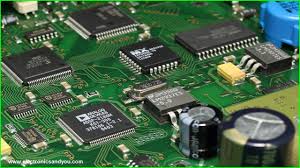
Can Circuit Board Be Used in IoT Devices?
The most efficient IoT PCBs are designed using advanced manufacturing techniques and cutting-edge materials. These methods, such as additive manufacturing and HDI technology, enable designers to optimize space utilization, enhance component integration, and overcome the limitations associated with size restrictions.
RF Connectivity: IoT devices frequently use a variety of wireless protocols to communicate with other devices and the cloud, including Zigbee, Bluetooth, Thread, and more. Proper RF design for IoT PCBs can help ensure that these devices have the lowest possible latency and highest level of signal integrity. This is accomplished by minimizing trace lengths, keeping critical analog components away from noisy digital ones, and implementing rigorous testing procedures.
Thermal Management: IoT devices are often battery powered and enclosed in slot-free cases, posing stringent thermal requirements. This can be addressed by selecting the right thermal interface material, using slotted holes for heat dissipation, and ensuring that all components are properly placed to prevent hot-spots.
It is important to select components that are compact, power-efficient, and have long lifespans for IoT PCBs. Additionally, careful attention must be paid to component placement to minimize signal interference and maintain proper spacing. It is also important to carefully consider the effect of EMI on IoT PCBs by designing antennas and implementing thorough EMI testing.
When it comes to sourcing PCBs for IoT devices, it is important to work with a trusted manufacturer that offers the latest technologies and manufacturing techniques. This will ensure that your IoT devices are built with the highest quality parts and assembled in a timely manner. Lastly, it is essential to use the right tools to analyze and test your IoT designs before they go into production. This will help to identify issues such as resist slivers and unintended copper exposed by solder mask, so that they can be corrected prior to fabrication.