
Manage Grounding in Flex Circuit PCBs
Grounding is a vital component of all PCBs. It ensures that signals get the proper voltage and current to operate correctly and safely. However, it’s even more critical in high-power and high-density flex circuit PCBs. This is because they’re prone to noise and interference from external electromagnetic (EMI) fields that can cause unwanted currents. As a result, effective EMI management is a must for ensuring your design is functional and safe.
Managing grounding in flex circuit PCBs can be difficult due to their complex layouts and limited rigidity. It’s important to have a good understanding of the various techniques that can be used to manage current flow and reduce EMI in these designs. These include using dedicated ground planes, conductive rings, and galvanic isolation. Incorporating these strategies into your flex circuit pcb layout is the best way to ensure it has proper functionality and safety.
A dedicated ground plane in a flex PCB is an essential tool for eliminating unwanted currents. It’s crucial to have a structure that can support the maximum currents and voltages your circuit requires while keeping them away from dangerous areas like the power supply. A dedicated ground plane can do this by providing a low impedance path for all signal conductors to get to their destination. It also helps protect the traces from EMI. In addition to using a dedicated ground plane, it’s essential to separate connectors by adding ground pins and routing them perpendicular to the overall bend. This minimizes stress and avoids copper breakage during bending.
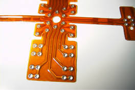
How to Manage Grounding in Flex Circuit PCBs
The thickness of a flex PCB’s copper layer is another factor that impacts its flexibility. A thicker copper layer makes it harder for the board to bend. Thinner layers, on the other hand, allow for greater flexibility. A mesh ground plane is a great option for flex and rigid-flex PCBs because it reduces the amount of copper while still providing adequate shielding.
However, a mesh ground plane is not without its drawbacks. While it provides a low impedance reference point, it can also radiate EMI due to open cavities in the flex ribbon. These EMI emissions can cause a problem with other devices that are connected to the same circuit.
To prevent this, it’s important to choose the right copper foil for your flex PCB. A higher-grade rolled annealed copper can be stretched further before fatigue cracking occurs and is more springy in the Z direction – exactly what you want for a flexible flex PCB.
When designing your flex PCB, be sure to keep the neutral bend axis as close as possible to the center of the stack to maintain balance and prevent destructive forces during bending. Additionally, be sure to avoid vias, cut-outs, slits, and holes in the bend area. These can increase stress and damage the copper. Finally, it’s also a good idea to stagger the traces on both the top and bottom of your flex PCB to avoid I-beaming. These overlapping traces can create an electric field that can cause signal degradation and circuit failures.