
high density interconnect
A high density interconnect is a technology that allows more components to fit in a smaller PCB. This makes it possible for engineers to create more complex electronic devices, while reducing their size and weight. This can be particularly important in areas where space and weight are limited, such as in portable consumer electronics or aerospace systems.
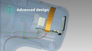
A high-density interconnect board is a printed circuit board (PCB) that has a higher number of layers and a greater wiring density than conventional PCBs. This allows engineers to use smaller components and create more complex electronic devices without compromising quality or functionality. These boards are also more durable, which is crucial for the demanding conditions that many electronic devices must withstand.
The key to a high density interconnect board is its multilayer construction. It is made from several layers of copper, with each layer having an insulating dielectric between them. This dielectric is essential to keeping the copper from touching each other and preventing shorting between adjacent layers. In addition, this dielectric offers thermal management capabilities, which help prevent overheating and improve reliability.
What is a high density interconnect?
The higher layer counts in a high-density interconnect PCB also allow for more components to be placed on both sides of the board. This is especially helpful in mobile devices like smartphones, which require more space for batteries and other power sources. The ability to accommodate more components in a smaller space also increases the efficiency of these devices by reducing their power consumption and increasing their speed.
High-density interconnect PCBs are also characterized by microvias, which are small holes that connect different layers. These vias can be created using a variety of methods, including laser drilling and photoresist deposition and exposure. The resulting patterns are then etched and cleaned, which removes the photoresist and leaves behind the conductor pattern. The via holes are then drilled and metallized, and the layers are stacked in multiple lamination cycles before outer layer processing.
Another feature of high-density interconnect PCBs is their enhanced thermal conductivity. This helps them dissipate heat more efficiently, enabling them to operate in a wider range of environmental conditions and ensuring that they maintain their optimal performance over time.
A wide variety of industries rely on high-density interconnect PCBs. The most common are telecommunications, where these boards are used to make routers and switches, and digital video and audio equipment, which often contain HDI PCBs. In addition, these boards are often used in industrial control panels and automation systems for facilities such as oil refineries and power plants.
The use of HDI PCBs allows manufacturers to produce more compact electronic devices with a lower weight and size, while still delivering the same level of performance as their predecessors. These benefits make HDI PCBs an indispensable tool for electronic engineers and enable them to develop cutting-edge products that can meet the demands of modern consumers.